Maskless Lithography: How it works

Maskless lithography is a next-generation microfabrication technique that projects digital light patterns directly onto a photoresist surface — removing the need for physical photomasks. The result is a faster, more flexible, and cost-efficient method for producing precise micro- and nano-scale structures.
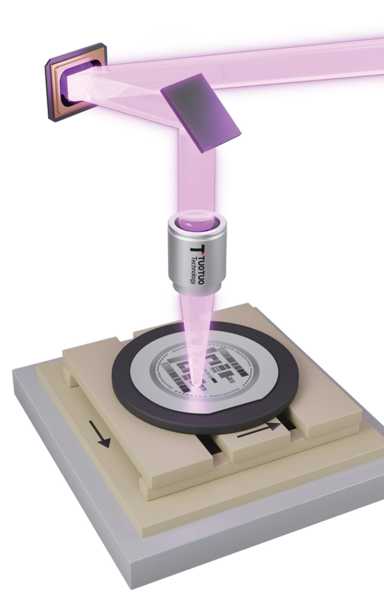
In a traditional photolithography process, a physical mask defines the pattern that UV light transfers onto a wafer.
In contrast, maskless lithography replaces this mask with a digital projection system.
A Spatial Light Modulator (SLM) or Digital Micromirror Device (DMD) converts computer-generated patterns into an optical image.
The UV light is reflected and focused through projection optics onto the photoresist-coated substrate, exposing it pixel by pixel.
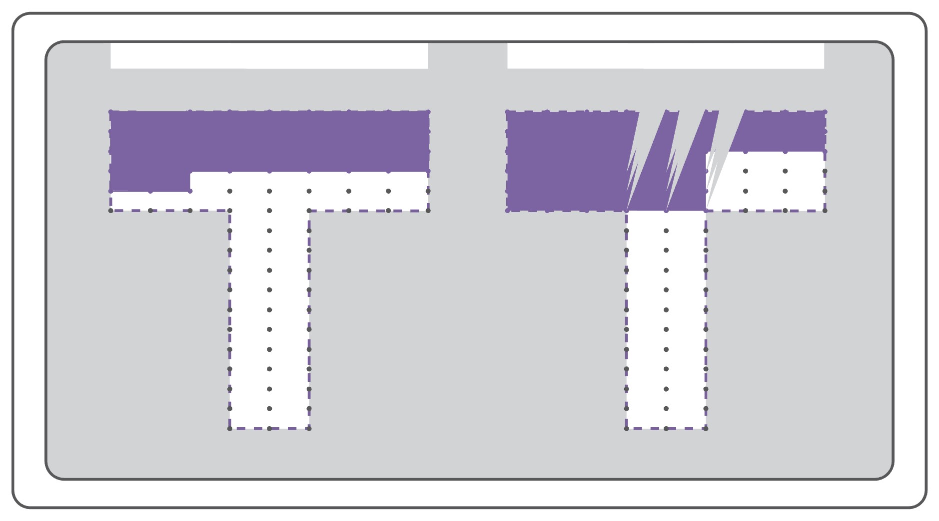
This digital approach allows instant pattern updates, real-time alignment correction, and fast design iteration — ideal for research, rapid prototyping, and small-batch production.
After exposure, the wafer undergoes development, where the exposed (or unexposed) photoresist areas are removed, depending on the resist type.
This reveals the precisely defined microstructures that can then be etched, deposited, or further processed to build microelectronic, photonic, or microfluidic components.
No photomask fabrication: Patterns are generated digitally.
Rapid iteration: Modify designs instantly for testing and optimization.
High precision: Sub-micron patterning achievable with advanced optics.
Cost-effective: Ideal for R&D labs and small-scale manufacturing.
Flexible substrates: Works with various materials, including silicon, glass, and polymers.
Maskless lithography is widely used in:
MEMS and sensor fabrication
Metamaterial and photonic crystal research
Microfluidics and biomedical devices
Semiconductor and display prototyping
For more details about the latest TuoTuo Maskless UV Lithography Systems, visit:
👉 TuoTuo Technologies – Maskless UV Lithography