3D Print in Microfluidic Device Fabrication

Microfluidic chips are a technology platform for precise control and manipulation of fluids at the micron scale (typically 1 micron to 1 mm in feature length). It is also known as "Lab-on-a-chip" because it uses microfabrication technology to highly integrate the basic operating units involved in the process of biological, chemical and medical analysis into a chip of only a few square centimeters or even smaller.
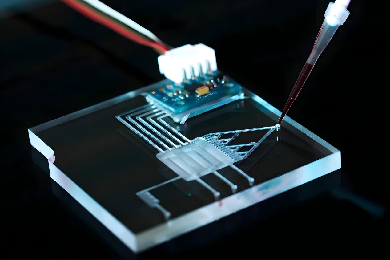
Light curing technology is one of the core technologies for the preparation of microfluidic devices by 3D printing, mainly including stereolithography (SLA) and digital light projection (DLP) two types, with high printing accuracy (10-100μm), fast curing, excellent surface quality, and moderate cost, it has become an ideal choice for printing complex structures, high-precision microfluidic devices (such as microreactors, micromixers, and integrated functional module devices), and its core applications can be carried out from two aspects: technical feature support and typical cases:
1. The adaptability of technical characteristics to the requirements of microfluidic devices
The core mechanism of light curing technology is to irradiate the photopolymer (composed of monomers, oligomers, and photoinitiators) through a specific wavelength (365-405nm) light source, initiate polymerization and curing, and then stack it along the Z axis through the printing platform to form a three-dimensional structure, as shown in the figure below.
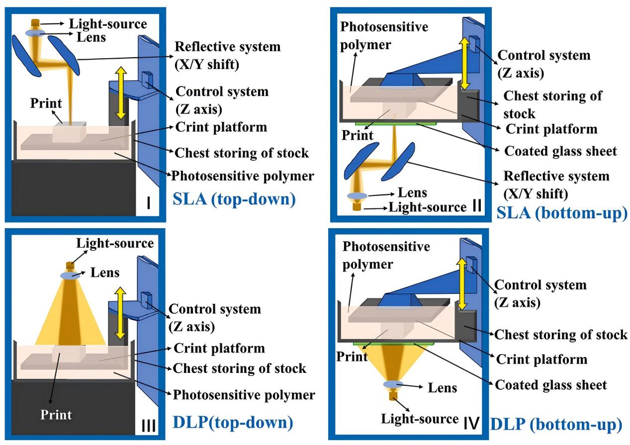
Schematic diagram of the working principle of light curing technology
This technology is naturally adapted to the needs of microfluidic devices:
1. High-precision and fine-scale manufacturing: It can realize sub-micron to micron-level microchannels (minimum 43μm) and complex runner networks (such as spiral and array hole structures) to meet the requirements of microfluidic "small-scale effect" for channel size (10-500μm). And the structural differences of different printing directions (top-down/bottom-up) can be selected according to demand;
2. Optical transparency: Photosensitive resins usually have high visible light transmittance after curing, supporting real-time optical monitoring of microfluidic devices (such as fluid flow observation and reaction process tracking).
3. Rapid prototype iteration: Fast curing speed (DLP can achieve surface curing), which can quickly verify the rationality of the flow channel design of microfluidic devices and shorten the R&D cycle.
4. Multi-material integration potential: Integrated printing of functional materials (such as insulating resin + conductive resin) can be realized through multi-resin switching, providing the possibility for microfluidic devices integrating sensing, catalysis and other functions.
2. Typical application cases
The application of light curing technology in microfluidic devices with different functions, covering chemical scenarios such as catalysis, nanomaterial synthesis, and separation, is as follows:
1. Multi-material and complex structure microfluidic device manufacturing
Quero team case: Developed a multi-material light-curing 3D printer, realized the switching and cleaning of more than 2 types of resins through the raw material tank tilt system and embedded peristaltic pump, and successfully printed a microfluidic chip with conductive electrodes - deposited 5 layers of 10μm thick conductive resin as electrodes between the insulating resin layers, and the minimum size of the prepared microchannels reached 43μm, which solved the problem that traditional single-material printing is difficult to integrate functional components.
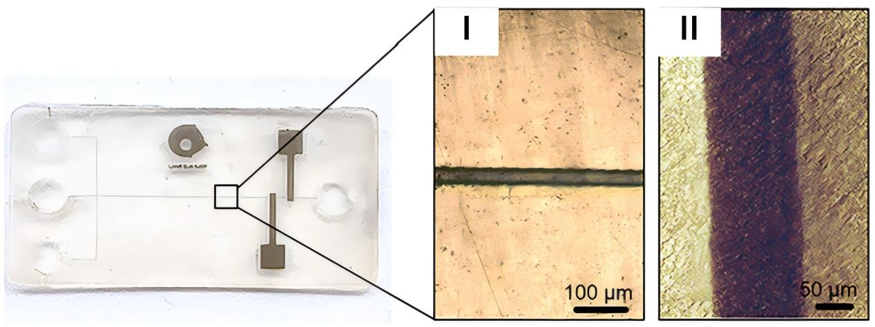
Optical microscopy of chip section and deposition of conductive resin
2. Micro-separation device manufacturing
Han team case: Using SLA-DLP composite light curing technology to prepare a microcyclone separator (μHC microreactor) with a size of only 250μm, the three-dimensional cross-section and physical diagram of the device are shown in the figure below.
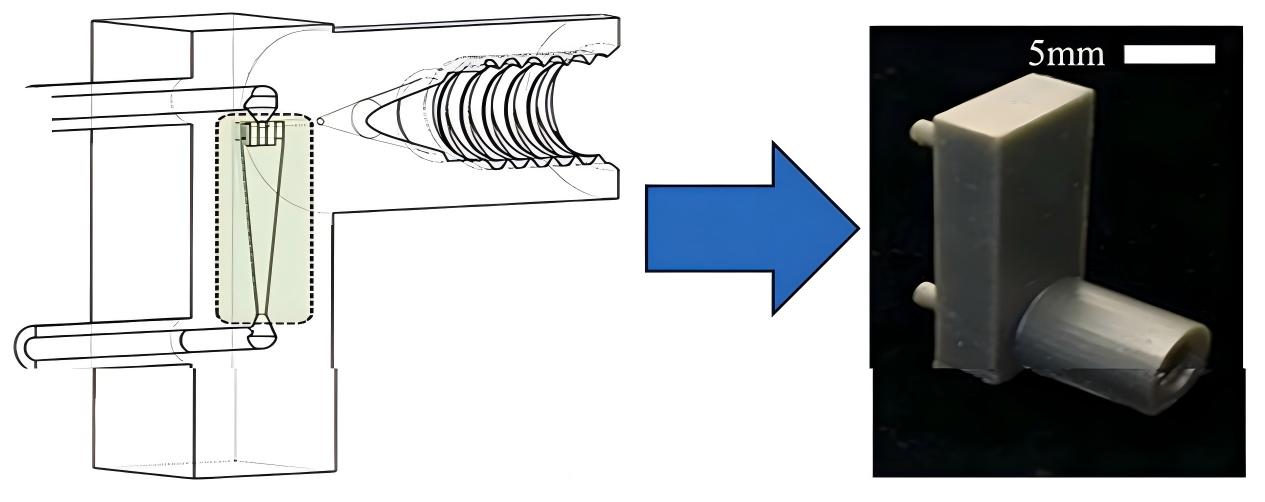
Three-dimensional cross-section of μHC microreactor based on light-curing molding and μHC microreactor photo
The device can efficiently separate sub-micron particles with a minimum separation size of 3.7μm, breaking through the limitations of traditional micromachining that is difficult to prepare miniaturized separation structures, and is suitable for the rapid separation of particles in trace fluids.
3. Catalytic reaction microreactor fabrication
Mei team case: Using photosensitive resin containing Al₂O₃/SiO₂ particles as raw material, carbon-ceramic composite microreactor with square, circular and diamond-shaped array pore structure is printed by SLA technology.
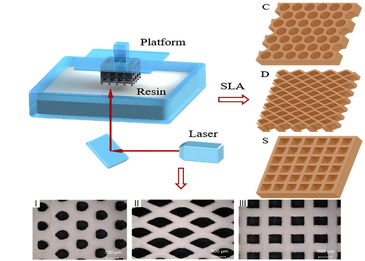
SLA printed geometric array structure and SEM diagram of pure ceramic microstructure at different resolutions
The specific surface area of the support was increased to 0.509m²/g (more than 7 times that of the traditional air sintering carrier), and the degradation efficiency of RhB reached 45.95% (1.97 times that of pure MoS₂) after loading the MoS₂ catalyst, and the efficiency remained at 82.35% after 5 cycles, which was suitable for environmental catalysis scenarios.
4. Nanomaterial synthesis microreactor fabrication
Riche team's case: Preparation of droplet microreactor using SLA technology using Somos Watershed XC 11122 photosensitive resin as raw material.
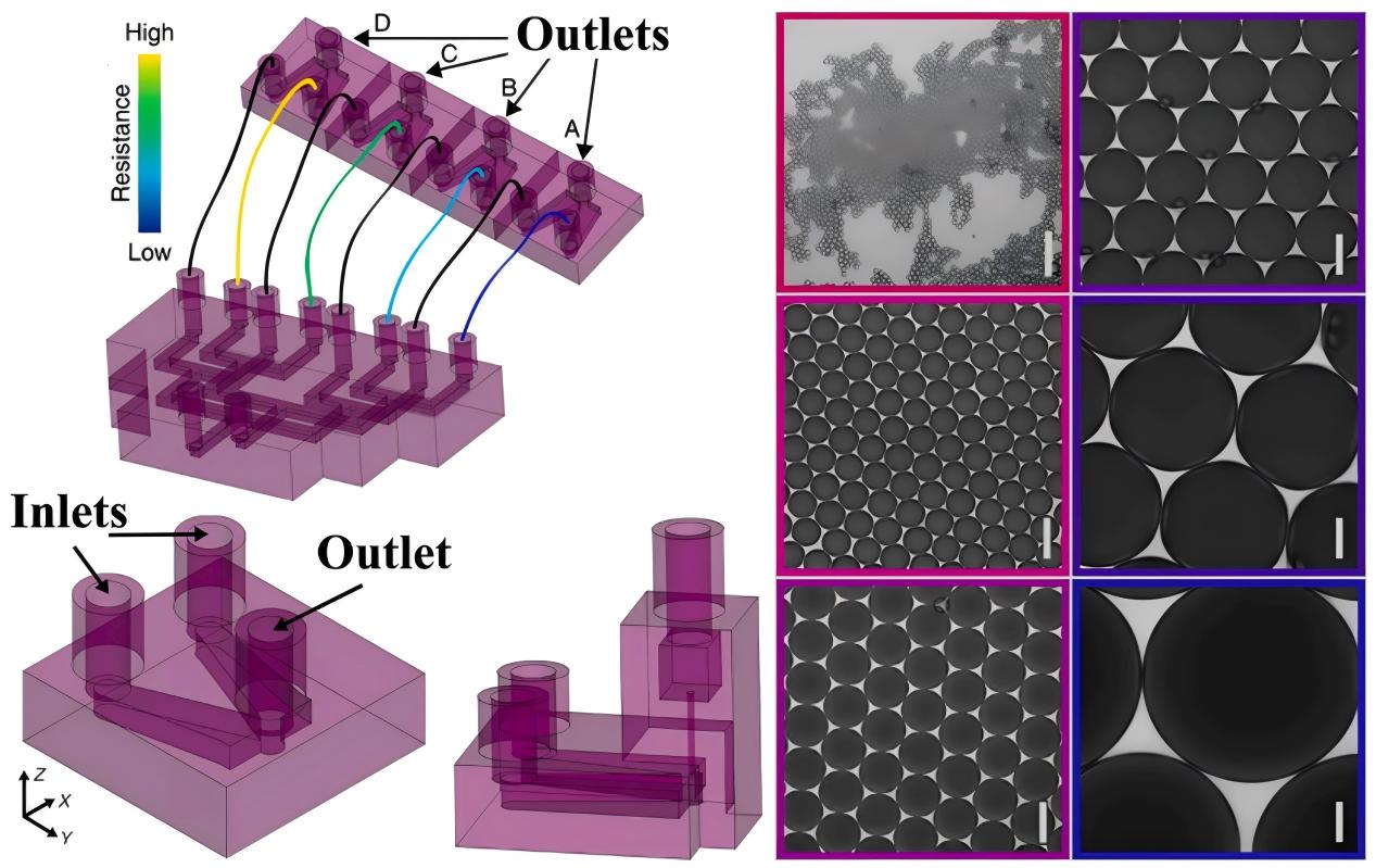
Schematic diagram of parallel components and individual droplet microreactors and photos of droplets of different sizes
Design 3D runners to achieve "flow-in-sensitive" droplet generation—even if the flow rate fluctuates, it can still produce single-disperse droplets (particle size spans up to 4 orders of magnitude), and support multi-channel parallel operation. When used for the continuous synthesis of platinum nanoparticles (Pt NPs), the reaction yield is nearly doubled compared with the traditional batch process, and the ionic liquid can be recycled three times to maintain purity and reactivity, while avoiding microchannel blockage through the droplet isolation mechanism.
Kumar team case: Fabrication of multi-layer integrated microfluidic chips using SLA technology
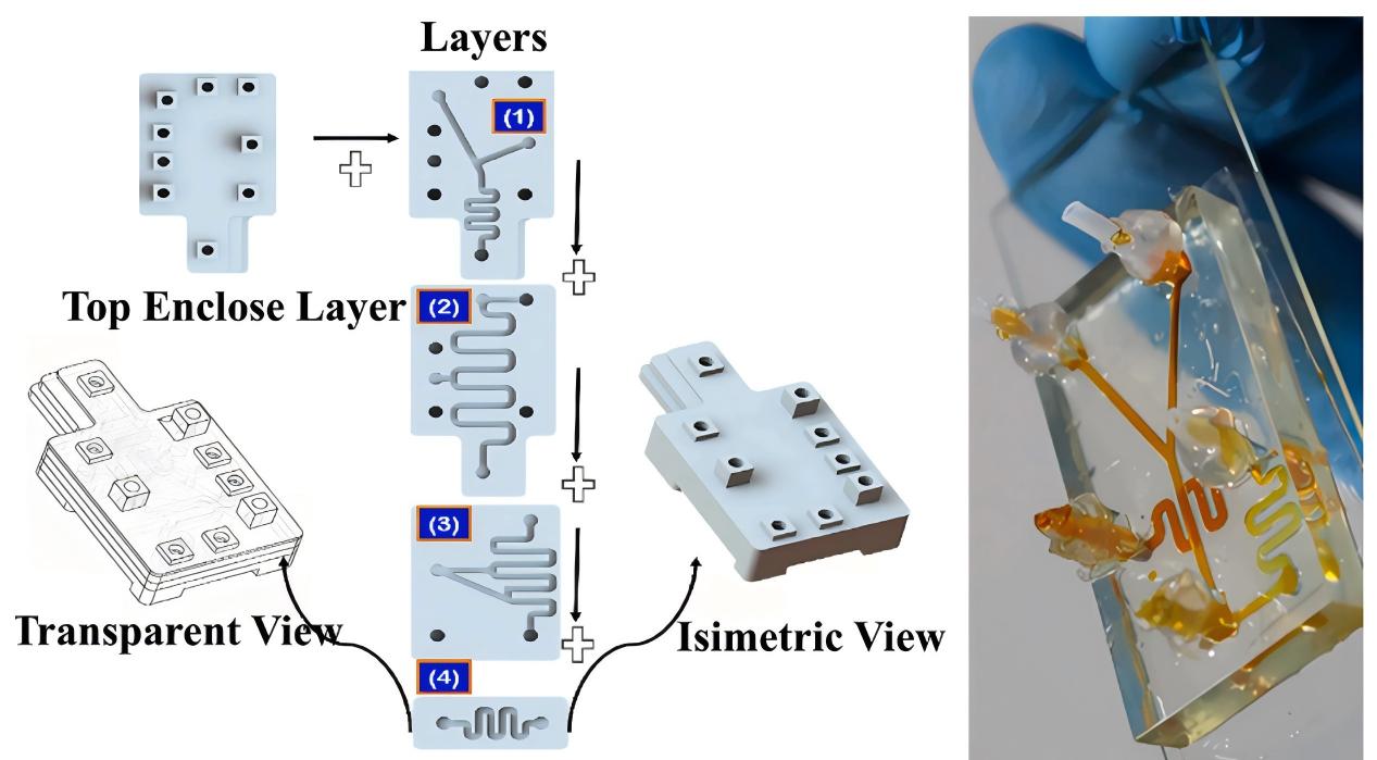
COMSOL simulation optimization diagram and physical photos of the internal channels and devices of the four-layer microreactor
The non-planar multichannel structure was designed to achieve the synthesis of sub-second (<1s) silver nanoparticles (Ag NPs) with an average particle size of 35nm without post-processing. Combined with multiphysics simulation and machine learning algorithms, the signal intensity of chemiluminescence sensing is increased by >1300%, and an intelligent prediction model of experimental parameters is also established, which is suitable for the integration of rapid nanosynthesis and intelligent sensing.
3. Key challenges in application
Despite the significant advantages of light curing technology in microfluidic device printing, it still faces some limitations:
Insufficient chemical stability: Most photosensitive resins are resistant to organic solvents, strong acids and alkalis, and are only suitable for mild chemical environments, and need to be improved by adding inorganic fillers (such as Al₂O₃, SiO₂) or composite modifications.
Process defects affect performance: light scattering can easily lead to "over-curing" and feature size broadening, and volume shrinkage during cross-linking will cause internal stress, causing device warping and delamination. The oxygen inhibition effect during "top-down" printing may cause the surface resin to not cure, and the residual raw materials of the microchannel need to be cleaned by ultrasound, stirring and other post-treatment.
Limited Mass Production: While suitable for rapid prototyping, the serialization of high-resolution printing, especially SLA, limits high-throughput production and requires technical optimization such as multi-nozzle parallelism.
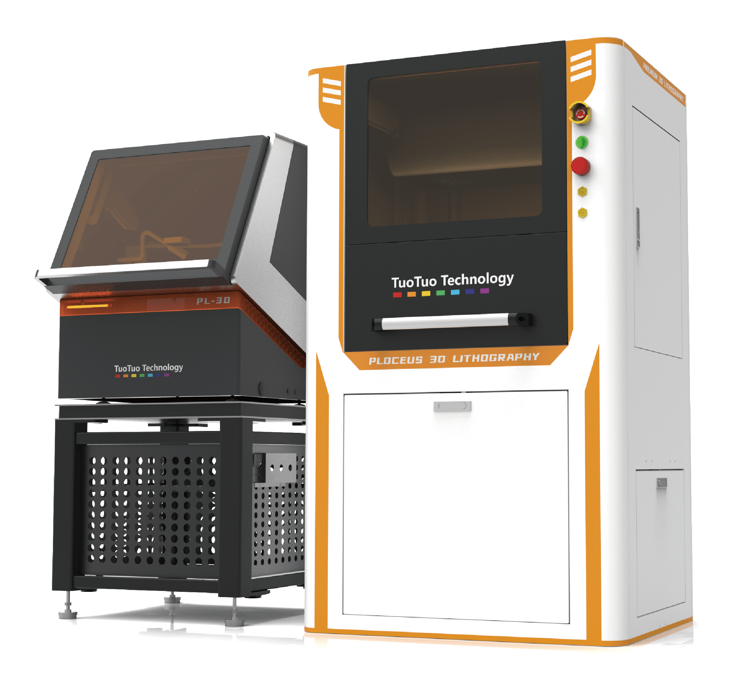
Weaver ® series ultra-high-precision 3D lithography equipment
Telephone: 400 856 0670
Email: marketing@tuotuot.com
The "Weaver ® Series Ultra-high-precision 3D lithography equipment" launched by Toto Technology has outstanding potential and advantages in the manufacturing of complex three-dimensional, high aspect ratio and composite three-dimensional micro-nano structures, with an optical accuracy of up to 1μm, a maximum processing size of 50mm×50mm×50mm, and printing materials compatible with conventional resins, Ceramic and hydrogel ink systems. The equipment has splicing printing technology, which can print the surface of existing structures for the second or multiple times, helping scientific research and industry to achieve a higher degree of design freedom and innovative breakthroughs in the field of micro-nano processing.