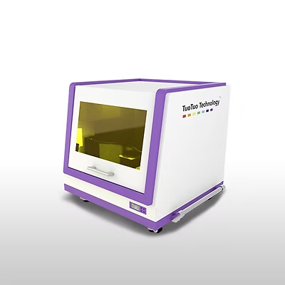
What is maskless lithography

Maskless lithography is an advanced microfabrication technique used to create patterns on substrates—such as silicon wafers, glass, or polymers—without the need for a physical photomask. Instead of projecting light through a patterned mask, this process directly writes the pattern onto the photoresist using a focused laser beam, electron beam, or digital micromirror device (DMD).
This approach provides unparalleled flexibility, precision, and cost efficiency, especially valuable for rapid prototyping, research, and small-batch production in fields like microelectronics, photonics, MEMS, and metamaterials.
In traditional photolithography, a mask acts as a stencil defining which areas of the photoresist are exposed to light. Creating a mask, however, can be expensive and time-consuming—especially when designs need frequent modification.
Maskless lithography eliminates this step by digitally projecting the pattern directly onto the substrate. Depending on the system, this can be done in several ways:
Laser Direct Writing (LDW):
A finely focused laser beam scans across the photoresist, exposing it point-by-point according to a digital pattern file (such as a CAD layout).
Digital Light Processing (DLP) or Grayscale Projection:
A DMD chip—containing thousands of tiny mirrors—projects the pattern as an image. Grayscale lithography can also modulate the intensity to produce 3D surface profiles with varying heights.
Electron Beam Lithography (EBL):
Instead of light, an electron beam exposes the resist, achieving resolutions below 10 nm. EBL is primarily used in research and semiconductor mask fabrication.
No Masks Required:
Reduces cost and lead time, ideal for R&D environments and custom device fabrication.
High Design Flexibility:
Patterns can be modified digitally and printed immediately—supporting rapid iteration and innovation.
High Resolution and Accuracy:
Modern systems achieve sub-micron or even nanometer-scale precision.
3D Structuring Capabilities:
Grayscale or multi-level exposure allows for the creation of micro-optical elements, diffractive structures, and metamaterial geometries.
Reduced Waste and Setup Time:
Digital workflows enable more sustainable and efficient prototyping.
Maskless lithography plays an increasingly central role in advanced material engineering and microsystem fabrication, including:
Micro-optics and photonics (e.g., diffractive optical elements, waveguides)
Metamaterials and plasmonic devices
MEMS/NEMS components
Biomedical sensors and lab-on-chip devices
Rapid prototyping for academic and industrial R&D
At Aralyse, maskless lithography—especially grayscale microfabrication—is an integral part of our micro- and nanostructuring capabilities. We use this technology to design and produce complex 3D microstructures for optical, sensing, and metamaterial applications, bridging the gap between materials science and functional device engineering.
Our team combines thin-film expertise, optical design, and process development to help clients move from concept to functional prototype with efficiency and precision.
Interested in custom micro- and nanostructuring solutions?
📞 +45 91 97 56 77
✉️ fekr@aralyse.tech
🌐 www.aralyse.tech